Nov 10 2017
For the first time, researchers at the University of Nottingham have developed a new, rapid method to 3D print fully functional electronic circuits.
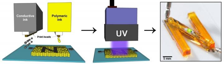 A schematic diagram showing how UV irradiation heats and solidifies conductive and dielectric inks to form the letter N with silver tracks that connect a green LED to a power source.(Credit: University of Nottingham)
The electronic circuits containing insulating polymeric inks and electrically-conductive metallic inks can now be developed in a single, unique inkjet printing process where the inks are rapidly solidified by UV light. The breakthrough method opens new avenues for the electronics manufacturing industry to develop fully functional electronic components, such as fully printed sensors and 3D antennae, from various materials including plastics and metals.
In the new technique, 2D printed electronics are combined with 3D printing or Additive Manufacturing (AM) – which is based on layer-by-layer deposition of materials to produce 3D products. This unique integration expands the scope of Multifunctional Additive Manufacturing (MFAM), in which various materials are printed in one additive manufacturing system to produce components with broader functionalities.
The latest technique overcomes some of the difficulties associated in developing fully functional devices that contains both metal and plastic components in complex structures, which can require different methods to solidify each material. The current generation of systems often use only one material which tends to restrict the functions of the printed structures. The range of functions in electronics can be expanded by having two materials like an insulator and a conductor. For instance, a wristband which is equipped with wireless communication circuitry and a pressure sensor can possibly be 3D printed and custom-made for the wearer in just a single process.
This advancement accelerates the solidification process of the conductive inks, reducing the time to less than one minute per layer. In the past, the same process took more time to complete with traditional heat sources such as hot plates and ovens which made it unfeasible when hundreds of layers are required to develop an object. Moreover, the development of electronic devices and circuits is reduced by present manufacturing methods that limit the form and possibly the performance of these devices.
Being able to 3D print conductive and dielectric materials (electrical insulators) in a single structure with the high precision that inkjet printing offers, will enable the fabrication of fully customized electronic components. You don’t have to select standard values for capacitors when you design a circuit, you just set the value and the printer will produce the component for you.
Professor Chris Tuck, Professor of Materials Engineering and also the lead investigator of the study
Printing fully functional devices that contain multiple materials in complex, 3D structures is now a reality. This breakthrough has significant potential to be the enabling manufacturing technique for 21st century products and devices that will have the potential to create a significant impact on both the industry and the public.
Professor Richard Hague, Director of the Centre for Additive Manufacturing (CfAM)
How it works
Dr Ehab Saleh and associates of the team from CfAM discovered that silver nanoparticles in conductive inks can efficiently absorb UV light. The heat produced from the absorbed UV energy evaporates the solvents in the conductive ink and eventually combines the silver nanoparticles. This procedure only impacts the conductive ink and does not affect the adjoining printed polymers. Using the same compact and low cost LED-based UV light, the researchers developed multi-material 3D structures by converting polymeric inks into solids within the same printing process
With technological developments, inkjet printing can deposit a variety of functional inks that have many properties. It is even employed in tissue bioprinting, biology, multienzyme inkjet printing, and many different forms of cell printing, where the ‘ink’ can contain living cells.
This breakthrough method has established a groundwork technology which holds immense potential in industry and academia. The study has paved the way for a number of collaborations to develop radio frequency shielding surfaces, medical devices, and innovative structures for harvesting solar energy.